
PCB Teasers: 11/01/13
This week in design: Breakout boards.
First, a SOIC-14 and SSOP-14 board. One on each side. It doesn't cost anything extra to have a design on the back, and gives two options for the price of one. Also note the fixes from my previous article regarding pin alignment (and also the longer pins for easier soldering).
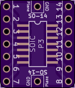
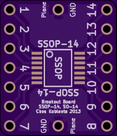


The next one was way more annoying to lay out...
I wanted an SOT-23 and SOT-323 breakout board. (I once made the mistake of using the wrong package - oops!) But when I was playing them, I realized that I could actually put two on each side. I tried two SOT-23 and three SOT-323 but couldn't route it on two layers; however, two SOT-23 and two SOT-323 worked. Figuring out how to route it was the hard part; after I connected the six pads on each side with vias, the rest was shockingly easy.
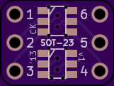
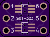


I also want a USB breakout. I was previously using the 10103593 in my designs, but found the 10118194 USB micro B socket. It's almost twice as cheap, and its tabs should actually go through the holes! The 10103593 had the bottom of its tabs aligned with the bottom of its surface - quite annoying, because it meant I had to physically bend things to fit, and they were still not really through the holes on the PCB, just barely in them. The datasheet shows this, and I should have paid more attention. Regardless, the 10118194 to which I am switching does not have these issues.
I also wanted my USB breakout to have some optional signalling. An LED when plugged in, and an LED for D+ and D-. The latter two will need to be connected with a solder bridge. Now, according to the spec, the differential lines swing to above 2.8V, and require a certain resistance (15K) to ground, or under 0.3V with a different resistance (1.5K) to 3.6V. I have no idea whether the LEDs on the lines will affect this. They very well may. So, we'll see!
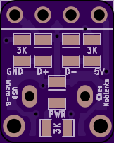
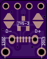


As you can see, I threw on a dual bidirectional TSV diode on the signalling lines. Like the other components, it's optional. That breakout board needs only a USB micro B receptacle, and a header or wires to break the signals out. I still don't know the best characteristics for a TSV diode for USB signal lines, so... whatever.
Also you can see the big trapezoids - those are where the solder bridges would go. (I decided that trapezoidal pads will be better for making bridges, but this is intuition and probably wrong! I haven't tested it.)
I also wanted a USB PCB that itself can be a plug - that is, that itself can be plugged right into a USB port. I looked at some USB plug datasheets, found some PCBs that do this, got some measurements, eyeballed a little, and made the plug. It's basically the same as the breakout board above, with the same components, except without a USB socket, but rather an extended PCB. (Also, how awesome would it be to put some flash memory and a USB-native flash controller, preferably with the media transfer protocol baked right in?)
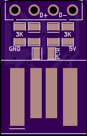
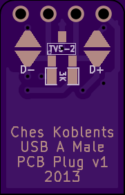


Up next: Breakout boards for BGA and QFN/QFP. I'll probably make one QFN/P, with one common pitch on each side; and one each for a common BGA pitch. I've thought about how to solder BGA without a heat gun / hot air rework station, and decided that I might be able to make this work with untented vias: place the chip on one side, heat and feed solder from the back. We will see how well it works!
Ches Koblents
November 4, 2013
November 4, 2013