
PIC SMD Tutorial: Circuit Design
This is part two of a six-part tutorial. The six parts will cover terminology, circuit design, component selection, board layout, board manufacturing, through-hole and surface-mount soldering, and embedded programming. The nature of this project allows a full lesson plan including all of these components, or any subset of lessons. Every lesson component is completely independent of the others, with the exception that soldering requires boards and components to be purchased, and programming requires at least the microcontrollers (and programmers) to be purchased. This tutorial is designed to teach surface-mount soldering using relatively simple components with large leads.
We will be using a PIC12F615 as the microcontroller. The circuit design and board layout is done using KiCAD. The microcontrollers are programmed with a Pickit (2 or 3), and the code is written in the MPLab X integrated development environment.
After the jump, we will discuss the requirements and the circuit designed to implement these requirements. Please open the definitions / terminology page in a new tab.
Requirements:
- Through-hole components to refresh soldering skills
- Surface mount components, hand-solderable with normal soldering iron tips
- Several package sizes, with slight decrease in size, to improve ability
- Programmable microcontroller
That leads us to some functional requirements, starting from the last point:
- Programmable microcontroller
- Programming interface accessible (broken out)
- All microcontroller pins accessible (broken out)
- Several I/O devices on-board; simplest: LEDs for output, pushbutton for input
The complexity of the requirements depends on the chip used. So I picked a chip I am comfortable using, with low complexity, excellent documentation, and a relatively cheap programmer: PIC12F615. It's 8-bit, has five I/O and one output, and eight pins. It comes in SOIC-150mil, which is easily hand-solderable. Perfect. Please open the PIC12F615 Datasheet.
Package (MCU)
If you want to skip this step, you can download the PIC12F615 component.
Let's get into the design. Fire up KiCAD, create a new project (from blank).
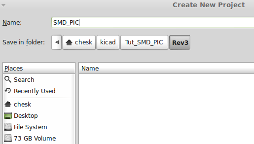

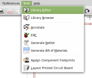
Open the schematic editor, then create a new custom library (or open one if you have one.)



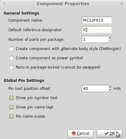
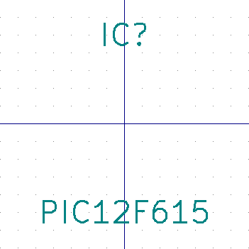
Create a device for the PIC12F615 based on the pinout on page 5 of the datasheet. You can zoom in by scrolling with your mouse scroll wheel.


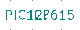


If you hover over an element, you can press a letter for an action. For example, mouseover the smushed text in the middle, and m will move it. You can also select the tools from the menus at the sides. With that, move the text away from the middle.

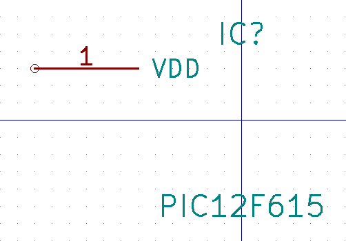
Now add the pins. Four on a side.
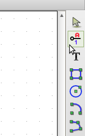
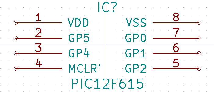


And add an outline. You should have a marking for either the first pin, or the top of the IC. I like to use a semi-circle. You can find the outline tools right below the pin button. After the outline, I like to reposition my reference to align with the left side of the outline.
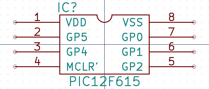
Finally, save the component into a new library. I named mine PIC12F615 (and you may download it if you're stuck or don't want to make your own component.)


Circuit
First, we need to add the new library to the list of used libraries.


Then add our device.
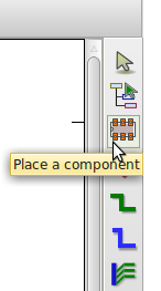
Once you have selected this tool, you should see your mouse become a pencil with crosshairs. Click somewhere in the middle of your page. Now you will see a dialog to add a component:
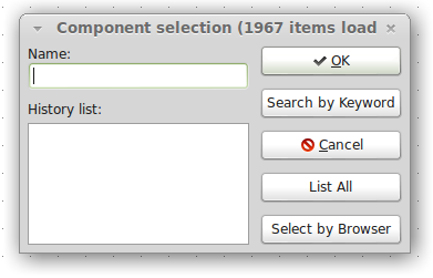
Now you can choose Select By Browser, browse to the library you added, and add the PIC12F615 part.

Once you have selected this tool, you should see your mouse become a pencil with crosshairs. Click somewhere in the middle of your page. Now you will see a dialog to add a component:

Now you can choose Select By Browser, browse to the library you added, and add the PIC12F615 part.
Next, add the power devices (+5V, GND).
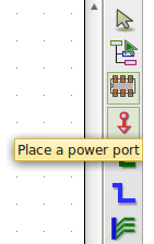

And hook them up!

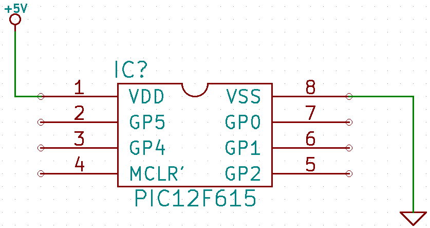


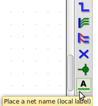
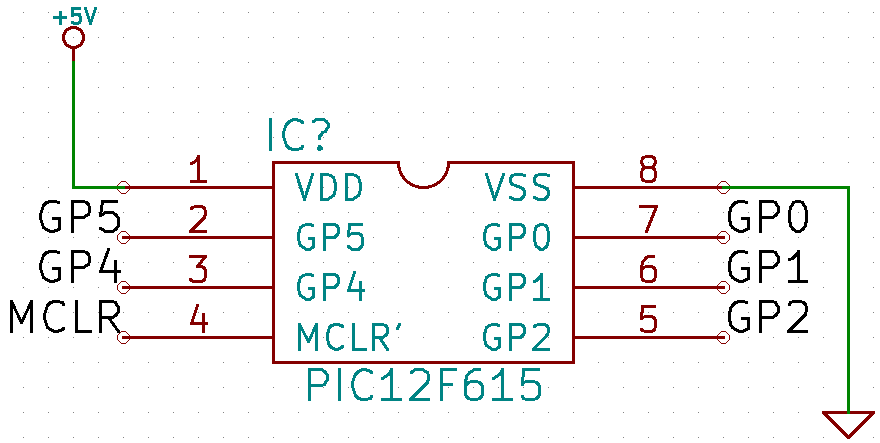
Now let's connect the rest of the I/O, and label everything. In KiCAD, as with most other tools, labeling a pin means assigning it to a net (a signal) - without necessarily using the wire tool. We will use the label button to name each connection.


Next, let's break out all the signals (break out, in this case, means wire all the signals so that they are easily accessible from the edges of the circuit board later). Eight pins, four on each side, just like the chip. We want to add CONN_4 devices from the conn (connector) library. Place each of the two headers in the schematic. Mirror one of them so that they are both facing the chip, with the first pin on the top (right click on the component, orient component, mirror vertically [Y]). Wire everything together.


Let's attach the programming interface. There are six pins, of which five are, in order: MCLR, VDD, VSS, PGD, PGC. In human terms, those pins are: memory clear / reset pin, positive power (+5V), ground, programmer data, programmer clock. You want to attach a 6-position connector, and connect the pins as stated above.
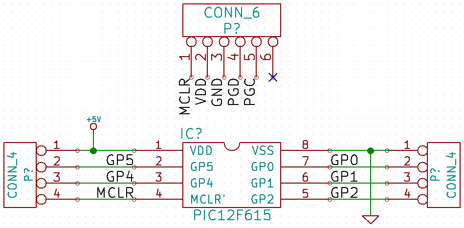
Now you want to look at the datasheet and figure out what those five signals correlate to. Obviously MCLR is MCLR and GND is GND, and we can see that VDD is +5V, but what do PGD and PGC correlate to? Wire it up and then check your work.
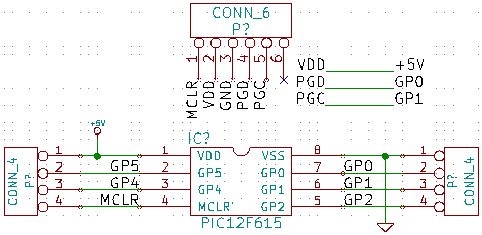

Now you want to look at the datasheet and figure out what those five signals correlate to. Obviously MCLR is MCLR and GND is GND, and we can see that VDD is +5V, but what do PGD and PGC correlate to? Wire it up and then check your work.

But aren't I missing something? For one, we have a recommended connection for MCLR (page 111). For another, there's always a recommended bypass capacitor between power and ground (0.1uF and 0.01uF in parallel, pages 157, 160).
The truth is, I've never had anything go wrong without these. I'm not putting this design anywhere important where 100% operation is absolutely critical. For the sake of simplicity, I'm ignoring these recommendations.
Next, let's attach I/Os mentioned above. I chose two LEDs and one pushbutton.
The LEDs have resistors in series (1k nominal, but frankly anything between 300 Ohms to 5K Ohms will probably work well enough; LEDs have a huge operating range for current.) These LEDs are driven with 5V signals and tend to have a 2V forward voltage, meaning the resistor drops the remaining 3V; at 1K, that's about 3mA per LED. I've had success operating these LEDs anywhere from 0.25mA to 25mA.
By the way, let's add LEDs to GP2 and GP4, and the pushbutton on GP5. Let's make the LEDs active-high (meaning we send a high signal to turn them on.)
By the way, let's add LEDs to GP2 and GP4, and the pushbutton on GP5. Let's make the LEDs active-high (meaning we send a high signal to turn them on.)
Pushbuttons are interesting. In theory, they create either an open or a short in the circuit. The signal should look like a step function. In practice, it wobbles up and down until it stabilizes. (You can see a reference image taken from an oscilloscope at pololu.com).
So if we create a bypass capacitor between the signal output and ground, we can alleviate this issue. We know there is an internal programmable weak-pullup resistor inside the pin at 20K ohms. (Page 152 shows 5V, 250uA typical current, and since .) If we choose a capacitor of 0.1uF (100nF), we get a time constant . That seems to be a big enough time constant to slowly change from high-to-low or vice-versa without the signal bouncing, yet small enough for a human not to notice a delay when the button is pressed.
V = IR, V/I = R, 5/0.000250 = 20000
T = RC = 0.0000001 * 20000 = 0.002 = 2ms
With the IO devices added (in the devices library), here's what the entire circuit looks like:
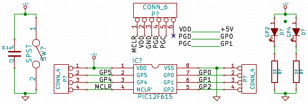

Next up: designing the circuit board.
Ches Koblents
January 17, 2014
January 17, 2014