Pic SMD Tutorial Rev1 Analysis
My first Osh Park design is very simple. I made a small learn-surface-mount-soldering tutorial:
- PIC12F615 - 8 pin SOIC
- Two 1k resistors - 1206
- Two LEDs - 1206
- Debounce capacitor - 1206
- Classic PCB pushbutton - through hole
- Two 4-pin headers, one on each side, for the PIC breakout
- One 6-pin ICSP (in-circuit serial programmer) header for PIC programming
So the total tally is: one SO-8, five 1206, and the rest through-hole. My next article will be about actually assembling, testing, and programming the little guy. But first, I'll go over issues I already see, and planned changes.
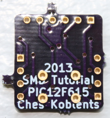
First, KiCAD has a bug where if you make a ground-ground via relying on ground planes, the data disappears, and you end up with just a via connecting nothing. You can clearly see the ground plane barely present on the back; a little in the middle, and almost entirely missing from the left and right.


However, you can see some vias that seem to connect nothing in those areas. Unfortunately, they were supposed to connect ground planes.
The solution is to connect vias with traces. The good news is that if you are planning to make a ground plane, you can obviously put down a ground trace, since there won't be any conflicts. The bad news is that I hope the ground signal to which you are connecting is close by. I've solved this issue in further revisions by having a really long ground trace connecting all the ground signals, then adding vias and ground planes later. This is annoying but such is life.
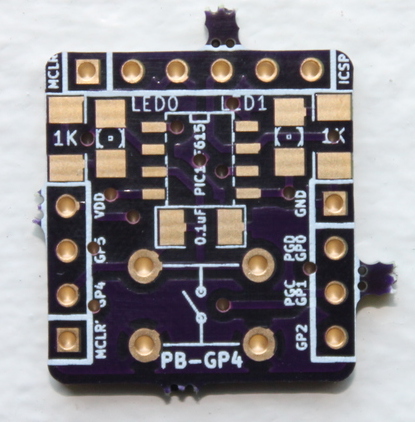
Second, you can see that the vias aren't tented! This makes the board look a bit ugly, since a bunch of the text is cut off. You can see this on the back above, as well as on the front:


I assume this is an issue on my end with gerber generation, but I will ask Osh Park how to fix it, since I can't figure out the problem. (The checkbox for 'do not tent vias' remains unchecked.) I will probably also decrease via size, since 35mil (0.035 inches) is rather large.
Third, I'd like to make the pushbutton surface mount as well.
Fourth, I should flip the left breakout so that the silkscreen shows pin 1 at the top, same as the right breakout.
Fifth, the LED 1206 footprint available in KiCAD has a tiny square indicating LED polarity on the silkscreen layer, but this did not translate to the actual printed silkscreen. I also don't like how the LED 1206 footprint is different from the general SMD 1206 footprint. To solve both of these issues, I will copy the SMD 1206 footprint to clearly indicate LED polarity and use that in the future.
Sixth, I'll have to wait until I solder one, but it's possible some components are too close. That was a risk I took. We'll see if it pays off!
Seventh change I'll consider: moving the PIC to the bottom of the board.
Eighth change: I may replace 1206 components with 0805, or even 0603. I may also mix and match by having some 1206, some 0805, and some 0603, so that there's a progression of skills learned.
There it is! Eight layout changes. Three bugfixes (two physical, one silkscreen), one possible bugfix due to positioning, and three possible improvements (more surface mount, smaller boards, and some smaller parts).
Finally, a process change! Back when dinosaurs roamed the earth, and it was only three years ago, surface-mount sockets were either prohibitively expensive or my google-fu was poor. Today, you can buy a SOIC-8 socket for $4 and a SOIC-16 socket for $8. (Technically, the SOIC-8 socket is a SOIC-16 socket with half the pins unusable). This is incredible, and it means that I can preprogram the PICs. I hadn't planned to do this but now I will.
Ches Koblents
September 20, 2013
September 20, 2013